This is an old revision of the document!
Table of Contents
Po-Hsuan_Wei
NOTOC<br>  <br> <br>BSEE: National Taiwan University, 2012-2013<br>MSEE: Stanford University, 2015-2016<br>Ph.D. Candidacy: 2014-2015<br>Email: pohsuan AT stanford DOT edu<br>LinkedIn: https://www.linkedin.com/in/pohsuanwei
Automated Layout Generation for Analog Circuits<br>
Layout is the Bottleneck of Analog and Mixed-Signal (AMS) Designs <br>
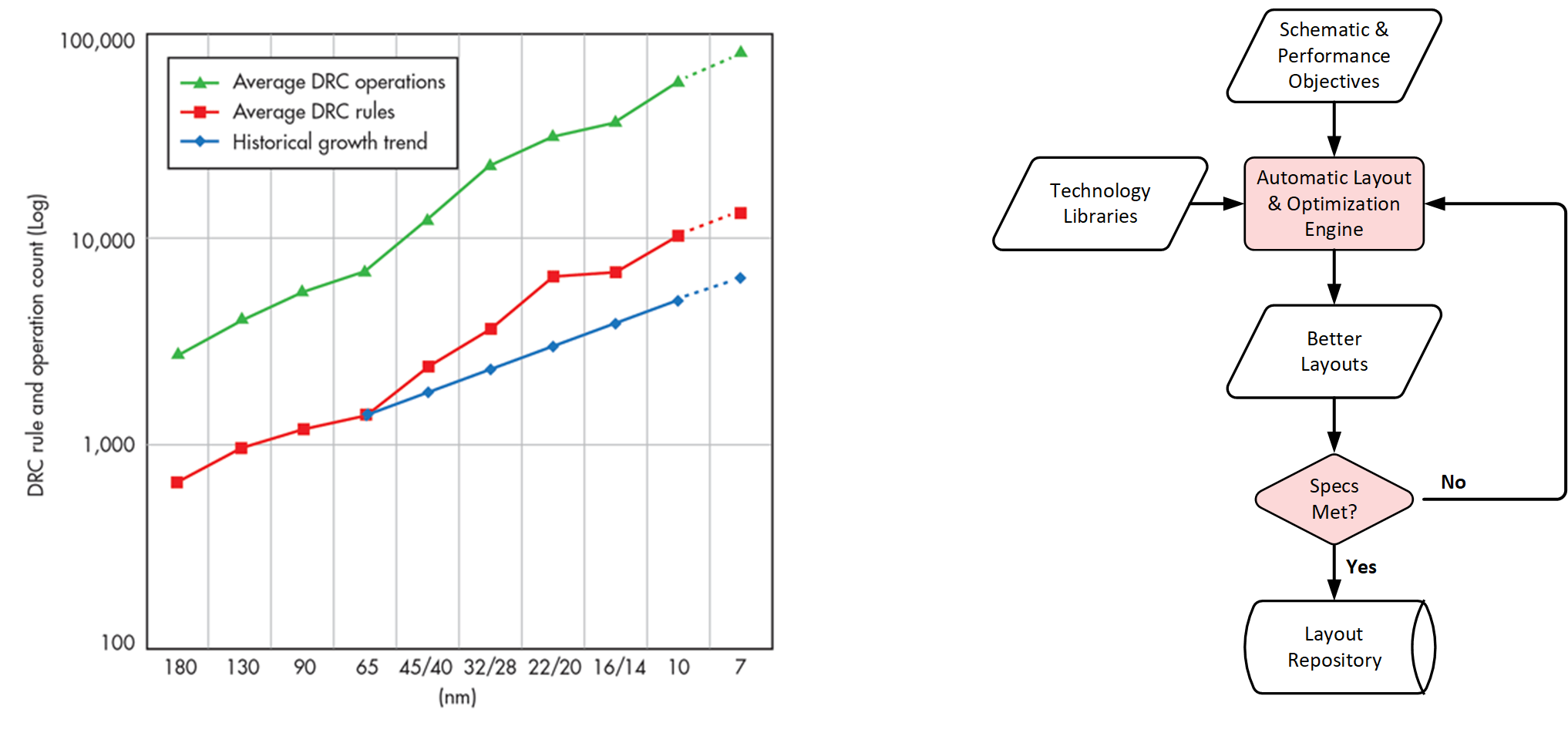
System-on-chips today are more than 80% digital 1. As digital components are the major part of the system, FinFET, with low leakage power and high operation speed, is highly favorable. While exhibiting the desired characteristics, the layout for FinFET has become more complex than ever. For one, the shrunken feature size mandates the use of more design rules, both in quantity and complexity. The back-end-of-line is fabricated with multiple patterning, which translates to metal coloring problem. Moreover, the routing is based on a grid-like layout with either horizontal or vertical direction for different metal layers, thus reducing the number of feasible solutions to circuit routing. Secondly, FinFET has severe layout-dependent effects, whose aggregated impact can only be observed from post-layout simulation. To increase the intrinsic gain, high stress is applied to the front-end-of-line, and thus the placement of the circuit components can greatly impact the characteristics of the devices. 2 The reduced wire width leads to higher resistance, causing voltage biases to degrade at an already low supply voltage. The inclusion of the middle-of-line layer and the 3D structure of FinFET inevitably increases the parasitic capacitance. The sheer number of design rules combined with significant layout-dependent effects results in several schematic-layout-simulation iterations, prolonging the turnaround time. In the case of AMS designs, where the layout is mostly done manually, such an iteration takes even longer to complete, and the designers have little power over the layout of their circuits.<br>
Automation Comes to the Rescue for AMS Designers<br>
Whereas the increased number of design rules is counter-productive for layout engineers, the reduction in the solution space is advantageous for rule-based automation tools. The considerable turnaround time and cost further justify the need for automating layout generation. Furthermore, automated layout generation gives AMS designers direct control over their own circuit layout and accelerates the iteration. These designers can not only optimize for their schematics, but also incorporate layout as part of the optimization process, which in turn produces higher quality ICs in a shorter time. <br>
Layout Generation Flow<br>
<span style=“font-size: 13.28px;”>Our approach aims to shorten and automate the iteration loop, preserve analog design intent systematically, leverage CPU power and free the engineers from having to labor over design rules. Moreover, our tool opens up the possibility of system-level layout optimization by producing multiple layouts with various performance profiles, all from the same schematic design. We have recently taped out a prototype IC using the proposed layout generation flow.</span>
<br>
 <br> Figure 1. Explosion of Design Rules 3 Figure 2. Proposed Automated Layout Generation Flow for AMS Circuits <br> <br> 1 P. Kinget, “Designing analog and RF circuits in nanoscale CMOS technologies: Scale the supply, reduce the area and use digital gates”, Proc. IEEE Int. Conf. Microwaves, Communications, Antennas and Electronics Systems, pp. 1, 2009 <br>2 K. -W. Su, Y. -M. Sheu, C. -K. Lin, S. -J. Yang, W. -J. Liang, X. Xi, C. -S. Chiang, J. -K. Her, Y. -T. Chia, C. H. Diaz, and C. Hu, “A scaleable model for STI mechanical stress effect on layout dependence of MOS electrical characteristics,” 2003, pp. 245–248.<br>3 http://www.electronicdesign.com/eda/are-you-really-ready-your-next-node