Table of Contents
Gift Nyikayaramba
BS, Electrical and Computer Engineering, Duke University 2015
MS, Electrical Engineering, Stanford University 2018
Admitted to Ph.D. Candidacy: 2016
Email: giftn@stanford.edu
Research: Low-power integrated interface circuits for structural health monitoring
$[hdcolor $\#80000$\$]
Background
$[/hdcolor$]
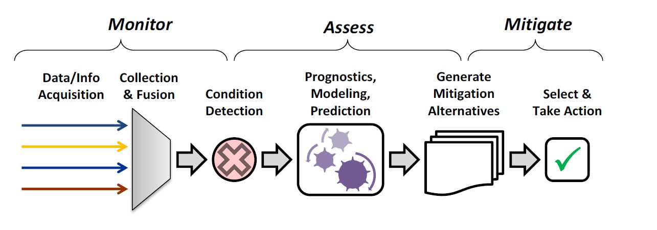
The ability to reliably detect, assess, and predict damage in critical aerospace, civil and mechanical structures is key to ensuring their safety and long-term maintainability.
Though effective, traditional non-destructive evaluation (NDE) methods involve the use of bulky equipment that makes automation and real-time, on-demand evaluations impossible. Furthermore, the growing prevalence of composite materials such as carbon fiber-reinforced polymer (CFRP) in aerospace engineering is driving a shift from the schedule-based monitoring and maintenance methods towards condition-based methods due to the complex failure modes that these composite materials exhibit.
Guided-wave structural health monitoring (SHM) enables the addressing of these challenges by employing networks of piezoelectric-sensors that are embedded within the structure under test. Ideally, the actuation and data acquisition electronics accompanying these embedded sensor networks should have a compact form factor that enables localized data collection and consolidation before communicating with the centralized processing unit that executes higher-level functions. However, despite advances in the sensors, the accompanying electronics have remained relatively bulky thereby greatly limiting the deployment of real-time, on-demand guided wave SHM.
$[hdcolor $\#80000$\$]
Integrated Interface ICs for SHM
$[/hdcolor$]
With aerospace applications as our target, the goal of our work is to design and implement integrated interface circuits to actuate and receive the guided Lamb waves that are used for SHM purposes. The miniaturization due to integration will, in turn, simplify the deployment of real-time SHM systems.
Prior integration efforts by our group resulted in the successful implementation of a four-channel, ±36 V, 780 kHz piezo driver chip 4. This chip uses a precisely-timed PWM driving scheme and it was designed and fabricated in a 0.25 micron BCD (Bipolar-CMOS-DMOS) technology. To enable more scalable integration of SHM ICs, the next challenge to be addressed is that of lowering the high actuation voltages (50-100 Vpp ) which are used in a typical SHM system in order to attain good receiver signal-to-ratio. These high actuation voltages are required because the diagnostic guided waves are highly attenuated due to propagation and conversion losses as they travel from one transducer to another. To provide these high actuation voltages, off-chip power supplies, costly high-voltage devices, and on-chip regulators are required and these increase die area and power consumption while limiting system scalability. My work focuses on implementing circuit and signal processing techniques to enable lower voltage actuation and more scalable integration of on-chip SHM systems
References:
[1]D. Rinehart, H. Jimenez, M. Blake and J. Nowinski, “Development of Real-time System-wide Safety Assurance Definitions and Concept Fundamentals”, 16th AIAA Aviation Technology, Integration, and Operations Conference, 2016.
[2]H. Boukabache, C. Escriba and J. Fourniols, “Toward Smart Aerospace Structures: Design of a Piezoelectric Sensor and Its Analog Interface for Flaw Detection”, Sensors, vol. 14, no. 11, pp. 20543-20561, 2014.
[3]X. Li, Z. Yang and X. Chen, “Quantitative Damage Detection and Sparse Sensor Array Optimization of Carbon Fiber Reinforced Resin Composite Laminates for Wind Turbine Blade Structural Health Monitoring”, Sensors, vol. 14, no. 4, pp. 7312-7331, 2014.
[4]Y. Guo, C. Aquino, D. Zhang and B. Murmann, “A four-channel, ±36 V, 780 kHz piezo driver chip for structural health monitoring”, 2013 Proceedings of the ESSCIRC (ESSCIRC), 2013.

